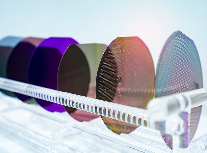
We provide silicon wafers and other types of bare wafers.
We sell dummy wafers with no particle guarantee, so please inquire if you are interested.
We also handle odd-lot inventory such as SOI wafers. Feel free to inquire.
| Conductive type | P/N |
|---|---|
| Crystal orientation | <100>/<111> |
| Resistance [Ω・cm] |
1 to 100 |
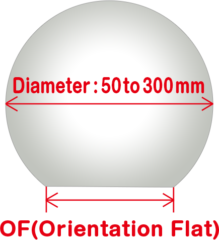
*OF length varies for different inch lengths.
*Both orientation flat and notch are available for 8-inch.
*Only notch is available for 12-inch.
| Size (inches) |
Diameter (mm) | |
|---|---|---|
| JEIDA | SEMI | |
| 2 | 50±0.5mm | 50.8±0.38mm |
| 3 | 76±0.5mm | 80±0.5mm |
| 4 | 100±0.5mm | 100±0.5mm |
| 5 | 125±0.5mm | 125±0.2mm |
| 6 | 150±0.5mm | 150±0.2mm |
| 8 | 200±0.5mm | 200±0.2mm |
| 12 | ー | 300±0.5mm |
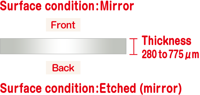
| Size (inches) |
Thickness (mm) | |
|---|---|---|
| JEIDA | SEMI | |
| 2 | 280±10mm | 279±25mm |
| 3 | 380±15mm | 400±25mm |
| 4 | 525±15mm | 520±20mm 625±20mm |
| 5 | 625±15mm | 675±20mm |
| 6 | 625±15mm | 675±20mm |
| 8 | 725±25mm | 725±20mm |
| 12 | ー | 775±25mm |
| Size (inches) |
OF (Orientation Flat) (mm) | |
|---|---|---|
| JEIDA | SEMI | |
| 2 | 17.5±25mm | 15.88±1.65mm |
| 3 | 22±2.5mm | 22.22±3.17mm |
| 4 | 32.5±2.5mm | 32.5±2.5mm |
| 5 | 42.5±2.5mm | 42.5±2.5mm |
| 6 | 47.5±2.5mm | 57.5±2.5mm |
| 8 | 57.5±2.5mm | 57.5±2.5mm |
| 12 | ー | ー |